
DF
Founded Year
2012Stage
Series C | AliveTotal Raised
$200MValuation
$0000Last Raised
$200M | 4 yrs agoMosaic Score The Mosaic Score is an algorithm that measures the overall financial health and market potential of private companies.
-132 points in the past 30 days
About DF
DF serves as an operator in the semiconductor industry. The company's offering is the production of single-crystal diamond wafers, which are used as a key component in various tech industries. These wafers are primarily sold to sectors such as AI and cloud computing, power electronics, and wireless communication. DF was formerly known as Paragon Mining and Diamond Foundry. It was founded in 2012 and is based in San Francisco, California.
Loading...
ESPs containing DF
The ESP matrix leverages data and analyst insight to identify and rank leading companies in a given technology landscape.
The diamond semiconductors market helps businesses access diamond semiconductors’ exceptional thermal conductivity, high breakdown voltage, and wide bandgap, which make diamond semiconductors ideal for high-power, high-temperature, and high-frequency applications. The unique properties of diamond enables the creation of highly efficient and reliable electronic devices that can operate under extrem…
DF named as Highflier among 7 other companies, including Power Diamond Systems, Great Lakes Crystal Technologies, and Okuma Diamond Device.
Loading...
Research containing DF
Get data-driven expert analysis from the CB Insights Intelligence Unit.
CB Insights Intelligence Analysts have mentioned DF in 2 CB Insights research briefs, most recently on Sep 23, 2024.
Sep 23, 2024
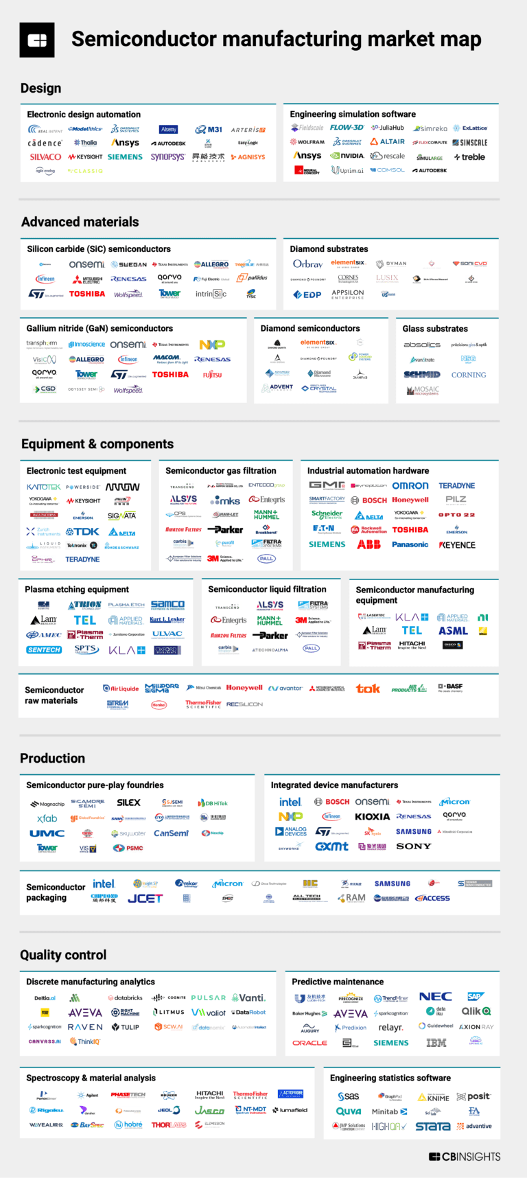
The semiconductor manufacturing market map
Expert Collections containing DF
Expert Collections are analyst-curated lists that highlight the companies you need to know in the most important technology spaces.
DF is included in 5 Expert Collections, including E-Commerce.
E-Commerce
11,341 items
Companies that sell goods online (B2C), or enable the selling of goods online via tech solutions (B2B).
Unicorns- Billion Dollar Startups
1,276 items
Luxury Tech
419 items
Tech-enabled companies launching new luxury brands, as well as startups providing tech solutions to the luxury industry, including e-commerce tools, marketing, and more. While these companies may not exclusively target luxury companies, they have notable luxury partners.
Semiconductors, Chips, and Advanced Electronics
7,380 items
Companies in the semiconductors & HPC space, including integrated device manufacturers (IDMs), fabless firms, semiconductor production equipment manufacturers, electronic design automation (EDA), advanced semiconductor material companies, and more
Artificial Intelligence
10,050 items
DF Patents
DF has filed 2 patents.
The 3 most popular patent topics include:
- hybrid electric buses
- hybrid electric cars
- hybrid powertrain

Application Date | Grant Date | Title | Related Topics | Status |
|---|---|---|---|---|
10/18/2018 | 3/1/2022 | Thin film deposition, Semiconductor device fabrication, Coatings, Plasma physics, Chemical processes | Grant |
Application Date | 10/18/2018 |
|---|---|
Grant Date | 3/1/2022 |
Title | |
Related Topics | Thin film deposition, Semiconductor device fabrication, Coatings, Plasma physics, Chemical processes |
Status | Grant |
Latest DF News
Jul 8, 2025
全球巨头押注“终极半导体”产业化 参与热点资讯讨论 金刚石作为一种超宽禁带 半导体材料 ,凭借其极高的热导率、高击穿场强、宽禁带等优异特性,在高功率、高频电子器件领域展现出巨大的应用潜力。近年来,随着 碳化硅 ( SiC )和 氮化镓 ( GaN )等宽禁带半导体的兴起,业界对性能更卓越的金刚石半导体寄予厚望,称其为“终极 功率半导体 ”。在这场颠覆性技术革命中,全球巨头正通过技术创新与战略合作加速布局。 元素六(Element Six) 同年9月,Element Six参与了美国国防高级研究计划局(D ARP A)主导的超 宽带 隙半导体(UWBGS)项目,利用其单晶金刚石 基板 开发面向军事和商业应用的新一代 半导体器件 ,旨在突破现有材料的性能极限。为支撑大规模应用,Element Six还建成并调试了一座由 可再生能源 驱动的先进CVD(化学气相沉积)生产设施,可批量生产高质量单晶金刚石衬底。 在产品创新方面,Element Six于2025年1月推出了一种铜-金刚石复合材料,结合了铜的高导热和金刚石的高热导特性,用于先进半导体器件的散热,其导热系数和热膨胀系数介于铜和金刚石之间,为高功率电子提供了新的散热解决方案。 此外,Element Six与Master Drilling公司合作,将其聚晶金刚石(PCD)切割技术应用于矿山和隧道掘进,提高了施工效率并降低环境影响。 Diamond Foundry 技术突破: 2023年10月,Diamond Foundry宣布成功培育出世界上首片直径100毫米(约4英寸)、重110克拉的单晶金刚石晶片。该晶片具有极高的热导率和电绝缘性能,被视为金刚石半导体材料领域的重大里程碑。公司宣称下一步目标是降低金刚石晶圆的缺陷密度,以实现比硅材料高约17200倍、比碳化硅高约60倍的品质因数。 同日,Diamond Foundry还发布了基于该单晶金刚石晶圆的 电动汽车 逆变器 “DF Perseus”,首批原型测试结果显示其体积比 特斯拉 Model 3的逆变器缩小了6倍,同时性能和效率均有提升。这一成果展示了金刚石材料在汽车电力电子领域的巨大潜力。 产能扩张与投资: 为加速金刚石晶圆的产业化,Diamond Foundry积极扩大产能并寻求政府支持。2024年12月,该公司获得欧盟提供的8100万欧元补贴,用于在西班牙特鲁希略市建设一座大型金刚石晶圆生产工厂。 据悉,该工厂总投资约8.5亿美元(约合62亿元人民币),计划于2025年投产,初期年产能可达400万至500万克拉单晶金刚石。工厂将采用先进的 等离子体 反应器 技术生产人造金刚石晶片,并有望成为全球首批完全由太阳能供电的绿色工业项目之一。 目前,Diamond Foundry已能在反应炉中培育出尺寸约4英寸、厚度小于3毫米的金刚石晶圆,可与硅 芯片 结合用于快速传导和释放芯片产生的热量。公司还开发了将金刚石以原子级直接键合到 半导体芯片 上的技术,以消除散热瓶颈,提升芯片性能。Diamond Foundry预计在2033年前后将金刚石材料大规模引入 半导体制造 领域。 Orbray株式会社 研发成果: 2021年9月,Orbray与日本佐贺大学合作,成功开发出直径2英寸的超高纯度金刚石晶圆。 2022年5月,基于上述2英寸晶圆,他们研制出输出功率高达875 MW/cm²、耐压达2568 V的金刚石半导体器件,创下当时全球最高纪录。这一系列突破使Orbray成为全球少数掌握大尺寸单晶金刚石生长技术的企业之一。 产业合作与规划: 为加速金刚石半导体的实用化,Orbray积极与产业界合作。2023年5月,该公司与 丰田 汽车旗下的车载半导体研发企业Mirise Technologies签署协议,共同研发垂直结构的金刚石功率半导体器件,以满足电动汽车对高性能功率电子的需求。根据协议,Orbray负责开发具有P型导电性的金刚石晶圆基板,Mirise则开发器件的耐压结构,双方预计金刚石功率半导体有望在10年内实现实用化。为此,Orbray计划投资100亿日元(约合5亿元人民币)新建一座工厂,用于生产车用功率半导体所需的金刚石晶圆基板,并同时量产 电动车 电子控制单元( ECU )等零部件。 2024年6月,Orbray与Element Six达成战略合作,联合生产“全球品质最高的单晶金刚石晶圆”,以服务6G通信、先进功率/射频电子、传感、热管理和量子技术等前沿领域。 同年9月,Orbray宣布计划筹资最多100亿日元,推动公司于2029年上市,并加强其秋田工厂的产能建设,目标是在金刚石和蓝宝石基板以及医疗业务的带动下,到2029年实现400亿日元的年营收。 2025年3月,Orbray宣布开发出世界上最大尺寸的自立单晶金刚石衬底(晶面为(111),尺寸20 mm×20 mm),并计划在2026年前将该技术商业化。这一成果进一步巩固了Orbray在大尺寸金刚石单晶生长领域的领先地位。 EDP株式会社 研发进展: 2023年,EDP成功开发出尺寸为10 mm×10 mm×0.2 mm的低电阻金刚石衬底(型号RB10102PP)以及更小尺寸的低电阻晶圆(RB13R2PP)。这些衬底通过在CVD生长过程中掺入高浓度硼元素,实现了高导电性,可用于高功率电子器件的研发。 2025年2月13日,EDP宣布研制出全球尺寸最大的单晶金刚石衬底,尺寸达到32 mm×31.5 mm。这一成果突破了此前大尺寸单晶生长的技术瓶颈,标志着金刚石衬底向更大尺寸迈进。 公司计划在2025年4月底前推出直径1英寸(25 mm)的金刚石晶圆,并在2025年底前通过拼接4块单晶的方式研制出直径2英寸(50 mm)的“马赛克”晶圆。 EDP还制定了更长远的目标:在未来2~3年内将单晶尺寸进一步提升至50 mm×50 mm,最终实现2英寸完整单晶衬底;若能突破50 mm见方单晶的生长技术,则可通过拼接4块这样的单晶来制造4英寸(100 mm)的马赛克晶圆。这一“逐步扩大、拼接成圆”的策略有望帮助EDP在较短时间内满足市场对大尺寸金刚石晶圆的需求。 日本住友电气工业 技术突破: 2025年3月,住友电工与大阪公立大学合作,在直径2英寸的多晶金刚石基板上成功制作出氮化镓(GaN)高电子迁移率 晶体管 (HEMT)。由于金刚石基板的热导率极高,该GaN器件的 热阻 大幅降低,仅为传统硅基板的1/4、碳化硅基板的1/2。 这一重要突破显著改善了高频无线通信GaN晶体管的散热性能,有望实现更高频率和更大输出功率的射频器件。该成果展示了金刚石基板在提升GaN基射频器件性能方面的巨大价值,也为 5G /6G通信、 卫星通信 等领域的 功率器件 发展提供了新思路。 业务布局: 作为综合性工业集团,住友电工在金刚石半导体领域的布局主要集中在材料和工具方面。除了上述GaN-on-diamond器件合作研发外,公司持续提供高品质的金刚石切割工具、研磨材料和散热基板等产品,支持半导体制造和 封装 过程中的精密加工与热管理需求。在金刚石单晶生长和应用方面,住友电工也保持着研发投入,以期在未来更广泛地将金刚石材料应用于功率电子和 光电子器件 中。 法国DIAMFAB 融资与合作: 2024年3月,DIAMFAB宣布完成了首轮870万欧元的融资,用于建立试验生产线,实现技术的预工业化,并加速产品开发以满足市场对金刚石半导体日益增长的需求。 同年12月,DIAMFAB与法国另一家CVD金刚石企业HiQuTe Diamond建立了战略技术合作伙伴关系。根据协议,DIAMFAB将负责利用先进的晶体生长工艺进行金刚石掺杂层的外延生长,并参与高性能金刚石器件的制造。这一合作整合了双方在金刚石材料制备和器件工艺方面的优势,有助于加快金刚石半导体从实验室走向产业化的进程。 技术进展: 作为初创公司,DIAMFAB目前的重点在于技术攻关和产品原型开发。据报道,公司已掌握了在大尺寸衬底上生长高质量金刚石外延膜的关键技术,并成功实现了金刚石的n型和p型掺杂,为制备金刚石 二极管 、晶体管等器件奠定了基础。DIAMFAB的金刚石材料有望用于制造高效率的功率 转换器 件(如逆变器、 变流器 ),帮助电动汽车提高能源利用效率、延长续航里程,以及用于绿色氢气生产中的高效电解 电源 等场景。随着融资的到位和合作的推进,DIAMFAB计划在未来几年内推出金刚石功率器件样品,逐步打开市场。 Coherent 2025年6月12日,公司重磅推出具有自主专利的金刚石-碳化硅陶瓷复合材料,这一成果堪称行业里程碑。该材料各向同性热导率突破 800W/mK,性能达到当前行业基准材料铜的两倍以上,同时其热膨胀系数与硅极为匹配,为直接与半导体器件集成提供了理想选择,有效解决了传统主流散热材料因各向异性结构导致的局部热积聚问题。 从产业投资布局来看,2024年4月,Coherent 宣布基于 CHIPS 法案获得1500万美元资金,用于加速下一代宽带隙和超宽带隙半导体(碳化硅和单晶金刚石)的商业化进程。 结语 金刚石半导体作为新一代半导体材料的代表,正在全球范围内掀起一场技术和产业的革新。从美日欧的产业巨头到新兴创业公司,都在这一领域投入资源、抢占先机。 当前,全球金刚石 半导体产业 格局初现:既有Element Six、住友电工这样的传统超硬材料巨头引领方向,也有Diamond Foundry、Orbray、EDP、DIAMFAB、Coherent等新锐企业加速追赶。在各方努力下,金刚石材料的制备技术不断取得突破,应用探索也日益深入。尽管面临成本和工艺等挑战,但在市场需求和政策支持的推动下,金刚石半导体有望在未来十年内迎来产业化的拐点。 可以预见,随着技术成熟和规模效应显现,金刚石半导体将在高功率、高频电子领域大展身手,成为推动能源高效利用和信息技术升级的重要引擎。展望未来,金刚石这一“终极半导体”的产业化之路虽非坦途,但前景值得期待。全球产业界和学术界需继续携手合作,攻克难关,共同迎接金刚石半导体时代的到来。 参考信息:本文部分素材和图片来自网络公开信息,本平台发布仅为了传达一种不同观点,不代表对该观点赞同或支持。如果有任何问题,请联系 19045661526(同微信)。 阅读全文 人工客服
DF Frequently Asked Questions (FAQ)
When was DF founded?
DF was founded in 2012.
Where is DF's headquarters?
DF's headquarters is located at 322 East Grand Avenue, San Francisco.
What is DF's latest funding round?
DF's latest funding round is Series C.
How much did DF raise?
DF raised a total of $200M.
Who are the investors of DF?
Investors of DF include Fidelity Investments, Future Tech Lab, Evan Williams, Jeff Skoll, Mark Goldstein and 13 more.
Who are DF's competitors?
Competitors of DF include LUSIX and 6 more.
Loading...
Compare DF to Competitors
Limelight Lab Grown Diamonds specializes in lab grown diamond jewellery. The company offers diamond-studded pieces, including rings, earrings, pendants, bracelets, and necklaces, crafted from lab grown diamonds and various metals. Limelight serves the luxury jewellery market. It was founded in 2019 and is based in Mumbai, India.
IIa Technologies is a company focused on lab-grown diamond technology within the gem and jewelry industry. The company's main service involves growing diamonds above the ground for various applications, using a sustainable process based on Microwave Plasma Chemical Vapor Deposition technology. These lab-grown diamonds are primarily used in the mechanical, high technology, and gem and jewelry industries. It was founded in 2005 and is based in Singapore.
Adamas Nanotechnologies specializes in the development and production of nanodiamond materials for various technology applications. Its products include fluorescent nanodiamonds, detonation nanodiamonds, and lubricant additives, all designed to enhance material properties and support advanced research. The company primarily serves sectors that require precision materials such as quantum sensing, biomedical imaging, and advanced manufacturing. It was founded in 2010 and is based in Raleigh, North Carolina.
FemtoSci focuses on advanced material technologies, specifically in the domain of functionalized diamond nanoparticles, within the materials science and electronics sectors. The company's main offerings include the development of additives for enhancing the thermal and mechanical performance of liquids and solids, as well as creating sensors, detectors, and microelectronic components designed to operate in extreme environments. FemtoSci's products are primarily utilized in the enhancement of thermal conductivity for transformer oils and plastics, and in the development of robust electronics for high-stress conditions. It was founded in 2012 and is based in Nashville, Tennessee.

DiamFab specializes in the development of diamond semiconductor technology for various industries. Their products are synthetic diamonds designed for electronics and extreme conditions, suitable for applications such as quantum computing. The company primarily caters to sectors that require advanced materials with high temperature, voltage, and radiation resistance. It was founded in 2019 and is based in Grenoble, France.

Carbodeon develops and supplies nanodiamond additives for industrial applications. The company offers nanodiamond-based products for metal plating, low friction coatings, and improvements in thermal and mechanical properties in polymers. Carbodeon's products are used in sectors such as oil and gas, where equipment reliability and operational efficiency are important. It was founded in 2006 and is based in Vantaa, Finland.
Loading...